Printed Circuit Board Drawing
Printed Circuit Board Drawing - Web printed circuit board designer post date. Web what is a pcb? Think of a pcb as a physical canvas or road map for designing electronic circuits. A printed circuit board is a rigid structure that contains electrical circuitry made up of embedded metal surfaces called traces and larger areas of metal called planes. Like most things in life, identifying components becomes easier when you break the task down into smaller parts. Web learn how to design a printed circuit board (pcb) and the standard workflow used in the industry. This allows components to be interconnected. Web pcb circuit diagram schematic board make relax tenang layout how can a printed circuit board help you test a circuit board schematic? Web a printed circuit board ( pcb ), also called printed wiring board ( pwb ), is a medium used to connect or wire components to one another in a circuit. This article explores the core principles of pcb layout, component placement, trace routing, signal integrity, and more. A printed circuit board is a rigid structure that contains electrical circuitry made up of embedded metal surfaces called traces and larger areas of metal called planes. Now, research presents a more durable printed circuit board that can. Web you need to create a printed circuit board so you can see it in action! Think of a pcb as a. How to make a printed circuit board (pcb) march 20, 2018 by suraj gehlot. Components are soldered to the board onto metal pads, which are connected to the board circuitry. Home page [people.ece.cornell.edu] schematics circuits termed electrical connections schematics. Whether your circuit is a project for school/college or is a final piece of electronics in a professional product for your. Is it a motherboard, a daughterboard, or does it perform a particular task? Pwm pins in the diagram have the same tilde sign in front of the pin numbers. Web a printed circuit board (pcb) is an electronic assembly that uses copper conductors to create electrical connections between components. Web one of the key concepts in electronics is the printed. Web learn how to design a printed circuit board (pcb) and the standard workflow used in the industry. Web printed circuit board designer post date. Web a printed circuit board is a bunch of electronic components interconnected via conductive paths printed on a baseboard. In this article, we will guide you through the entire process of designing a pcb, covering. Web learn how to design a printed circuit board (pcb) and the standard workflow used in the industry. How to make a printed circuit board (pcb) march 20, 2018 by suraj gehlot. Components are soldered to the board onto metal pads, which are connected to the board circuitry. Web what is a pcb? This tutorial will breakdown what makes up. Web a printed circuit board (pcb) layout is the blueprint that guides the production of circuit boards which are the backbone of any electronic device. Home page [people.ece.cornell.edu] schematics circuits termed electrical connections schematics. Now, research presents a more durable printed circuit board that can. Read on to learn the universal pcb design steps. Experience in drawing electrical schematics benefit. Pwm pins in the diagram have the same tilde sign in front of the pin numbers. Web a printed circuit board is a bunch of electronic components interconnected via conductive paths printed on a baseboard. Web to design a printed circuit board (pcb), you need to draw holes, pads, and wires for your circuit. Web what is a printed circuit. Web a printed circuit board (pcb) layout is the blueprint that guides the production of circuit boards which are the backbone of any electronic device. Web what is a printed circuit board? Web a printed circuit board ( pcb ), also called printed wiring board ( pwb ), is a medium used to connect or wire components to one another. Web a printed circuit board ( pcb ), also called printed wiring board ( pwb ), is a medium used to connect or wire components to one another in a circuit. Web printed circuit board designer post date. This allows components to be interconnected. Components are soldered to the board onto metal pads, which are connected to the board circuitry.. Web one of the key concepts in electronics is the printed circuit board or pcb. In this article, we will guide you through the entire process of designing a pcb, covering the fundamentals to creating the final artwork. Home page [people.ece.cornell.edu] schematics circuits termed electrical connections schematics. Web in this kicad tutorial for beginners, you'll learn to make your first. These boards are also called substrates. In an age of rapid change, the pcb industry is. A printed circuit board is a rigid structure that contains electrical circuitry made up of embedded metal surfaces called traces and larger areas of metal called planes. This tutorial will breakdown what makes up a pcb and some of the common terms used in the pcb world. Web learn how to design a printed circuit board (pcb) and the standard workflow used in the industry. Web you need to create a printed circuit board so you can see it in action! From design to final artwork. Web pcb design is the process of designing printed circuit boards (pcbs) with an assembler in order to assemble electronic circuits. Instead, it is a systematic process that starts from capturing the requirements of the design to testing out the finished prototype. Web a printed circuit board (pcb) is an electronic assembly that uses copper conductors to create electrical connections between components. We provide aluminum pcbs for all your led lighting needs. Now, research presents a more durable printed circuit board that can. Web in this kicad tutorial for beginners, you'll learn to make your first printed circuit board (pcb). If you are into electronics, pcbs are some of the most common things you will see. Web if your board has no printed labels, check out its pinout diagram documentation (found on the board's arduino store page). In this article, we will guide you through the entire process of designing a pcb, covering the fundamentals to creating the final artwork.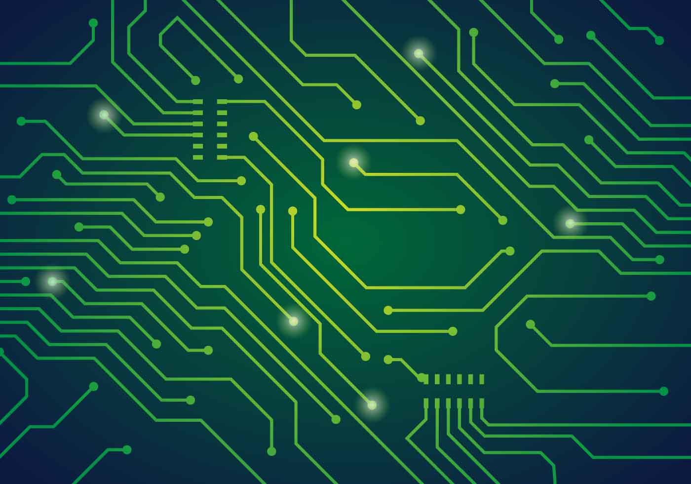
Printed Circuit Board Vector Illustration 344822 Vector Art at Vecteezy
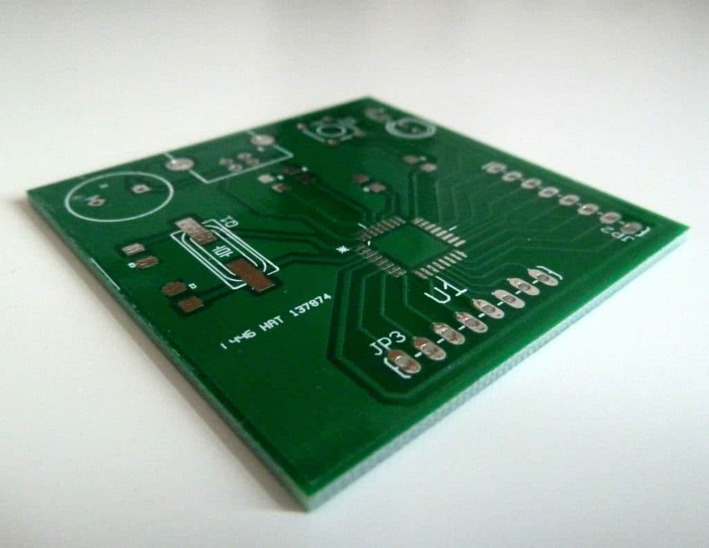
Printed Circuit Board Guide For Beginners Build Electronic Circuits
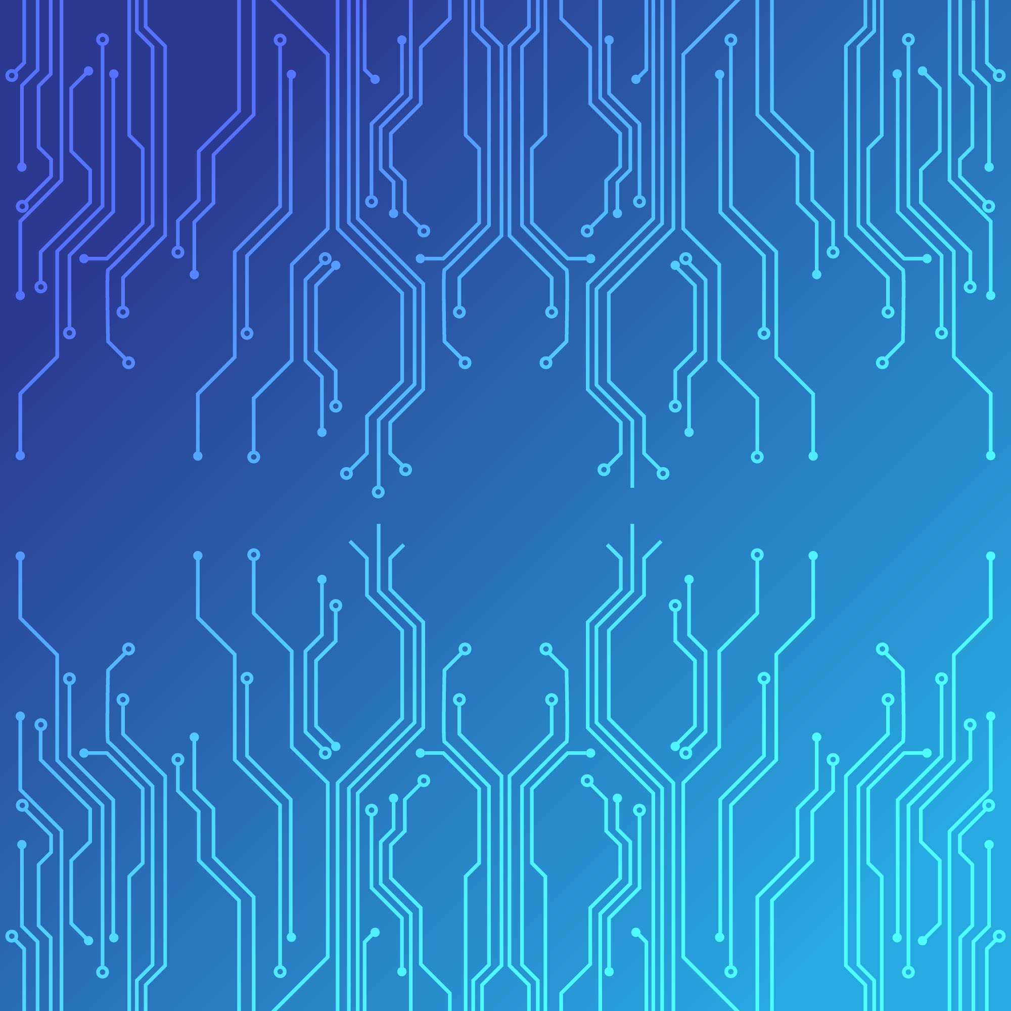
Printed Circuit Board Vector 338569 Vector Art at Vecteezy
printed circuit board drawing Wiring Diagram and Schematics
Printed Circuit Board (PCB) Design CIRCUITSTATE Electronics
Printed Circuit Board Vector 343900 Vector Art at Vecteezy

Printed Circuit Board Design, Diagram and Assembly Steps & Tutorial
Printed Circuit Boards

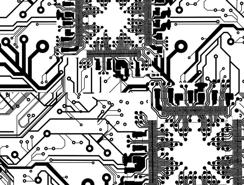
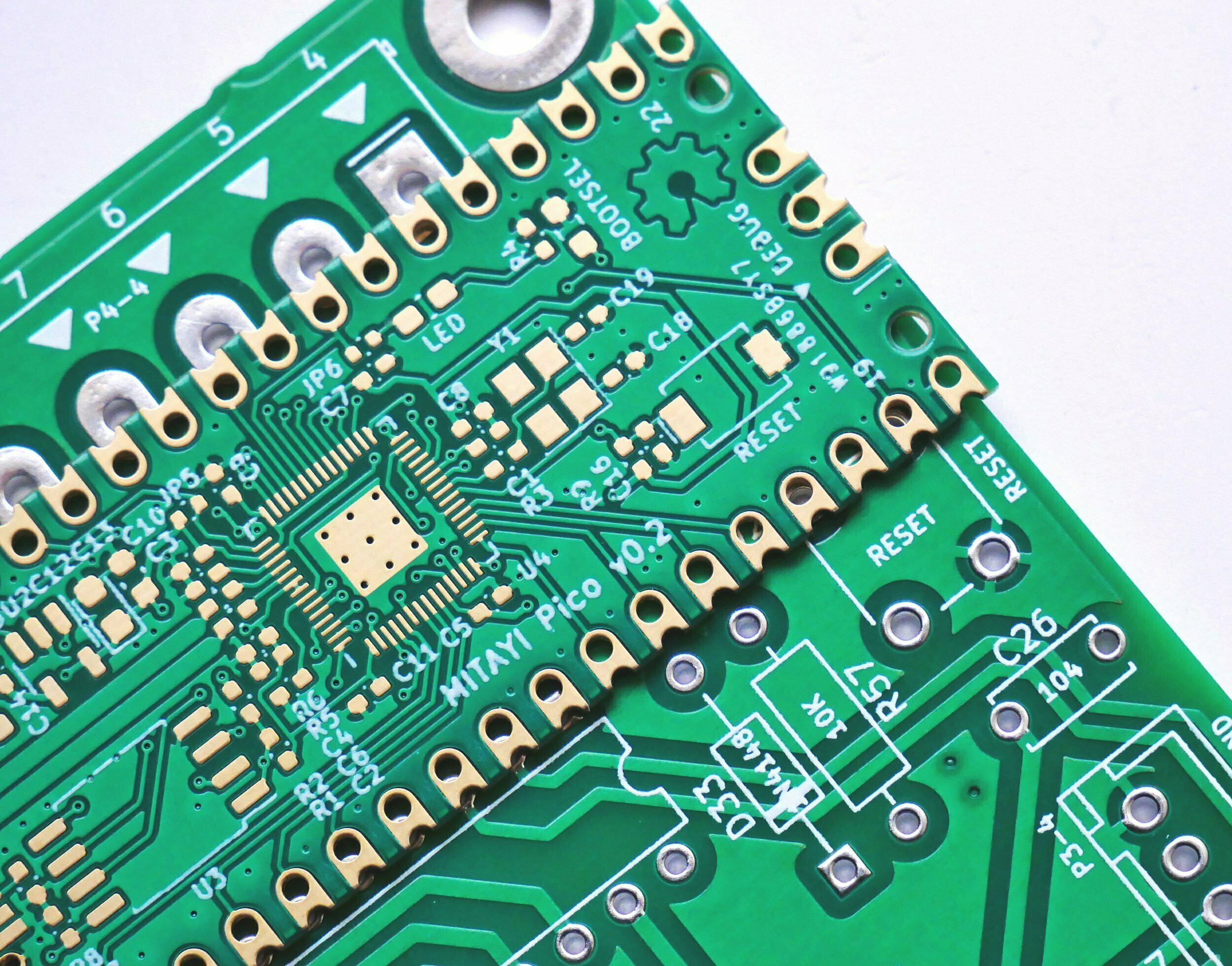
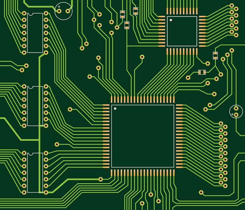
How To Read Printed Circuit Board Diagram
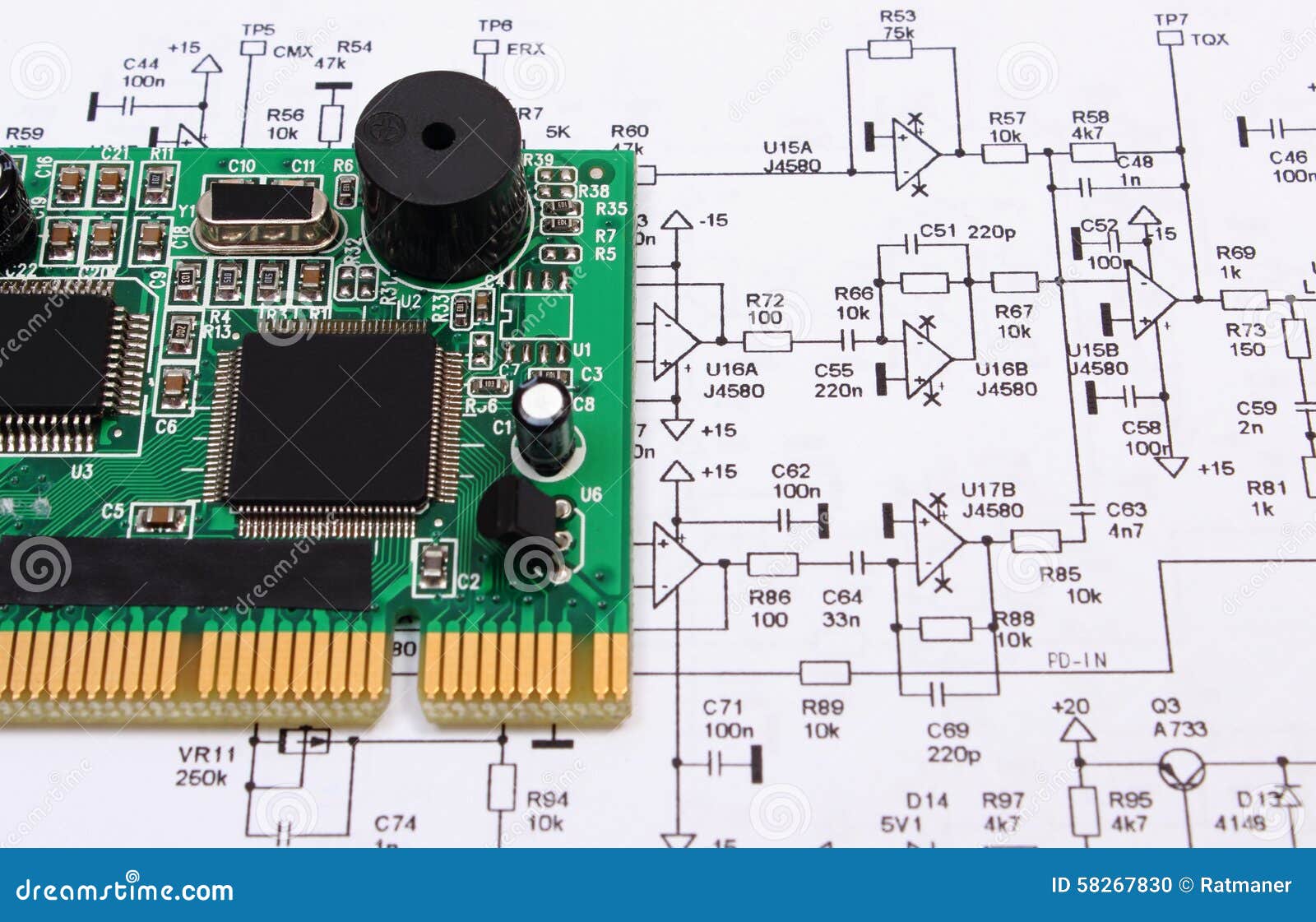
Printed Circuit Board Lying on Diagram of Electronics, Technology Stock
Components Are Soldered To The Board Onto Metal Pads, Which Are Connected To The Board Circuitry.
This Block Diagram Is Converted Into A Schematic Design Using A Cad Software.
Web Printed Circuit Board Design Begins With The Creation Of A Conceptual Block Diagram.
Web Pcb Design Is More Than Putting Together A Few Components And Drawing Traces Linking Them Together.
Related Post: